

Semiconductor Wafer Solutions
Click to explore wafer-level testing solutions
Through our global network of testing experts and analytical equipment including chromatography (HPLC, GC, GC/MS) and atomic absorption spectroscopy (AAS, GFA, FIAS), Our goal is to provide test services as efficiently as possible to maximize our customers' profits. For more information about our services, contact one of our experts today.
Note: this service is for Research Use Only and Not intended for clinical use.
A semiconductor is a material that has a conductivity between the conductor and the insulator. When it is stimulated by external light and heat, the electrical conductivity will vary significantly. By adding a small number of impurities to a pure semiconductor, the conductivity is drastically increased. It is precisely the various semiconductor properties of semiconductor materials that impart different functions and characteristics to various types of semiconductor devices.
Alfa Chemistry's semiconductor testing services provide valuable answers to clients around the world, and our experienced experts can provide you with complete turn-key semiconductor design, development, qualification, test development and production support services that are second to none.

Optoelectronic semiconductor
Optoelectronic device
Discrete device
Sensore
Wafer probers
Component handlers using ATE (Automatic Test Equipment)
High temperature testers
Qualification and failure analysis
ASTM
As a reliable third-party testing company, Alfa Chemistry provides Material testing services to clients around the world to ensure the quality and safety of your products. With a professional analysis team and advanced instruments, we provide you with the most accurate testing results in the shortest time possible. To learn more about our services, please feel free to request a quote or consult our experienced scientists.
Oscilloscope
Used to measure the waveform, frequency, amplitude, and other parameters of electrical signals.
Multimeter
Measures basic electrical parameters such as voltage, current, and resistance.
Spectrum Analyzer
Detects the spectral characteristics of signals.
Semiconductor Parameter Analyzer
Measures various parameters of semiconductor devices.
Probe Station
Used for testing chips.
X-ray Inspection System
Detects the internal structure and defects of packaged components.
Optical Microscope
Observes the surface morphology of samples.
Atomic Force Microscope (AFM)
Provides higher-resolution surface morphology information.
Energy Dispersive Spectrometer (EDS)
Analyzes the composition of materials.
Reliability Testing Equipment
Includes high-temperature, low-temperature, and vibration testing devices to assess the reliability of semiconductor devices.

 Lamuta, Caterina, et al. Journal of Physics and Chemistry of Solids 116 (2018): 306-312.
Tin selenide (SnSe) has emerged as a promising material for flexible electronics due to its remarkable mechanical properties. This case study reports the direct evaluation of its mechanical characteristics through nanoindentation experiments, focusing on determining its Young's modulus and hardness. The tests reveal that SnSe possesses a Young's modulus of 25.3 GPa and a hardness of 0.82 GPa, providing critical insights into its suitability for flexible applications.
Nanoindentation experiments were conducted using the continuous stiffness measurement (CSM) method with varying loads. Initially, the indentation curve showed no damage, indicated by the absence of pop-in events, ensuring that the material remained intact during testing. As the penetration depth increased, both Young's modulus and hardness stabilized at approximately 25 GPa and 0.8 GPa, respectively, for depths up to 400 nm. However, deeper penetrations resulted in a decrease in hardness, accompanied by pop-in events, signaling material damage.
These findings are crucial for understanding the mechanical resilience of SnSe in real-world applications. The data confirms that SnSe maintains excellent mechanical properties under moderate stresses but may experience degradation under deeper indentations, emphasizing the importance of load management in its practical use in flexible electronics.
 Aguilar-Burgoin, Hector Alfredo, et al. Available at SSRN 5030832.
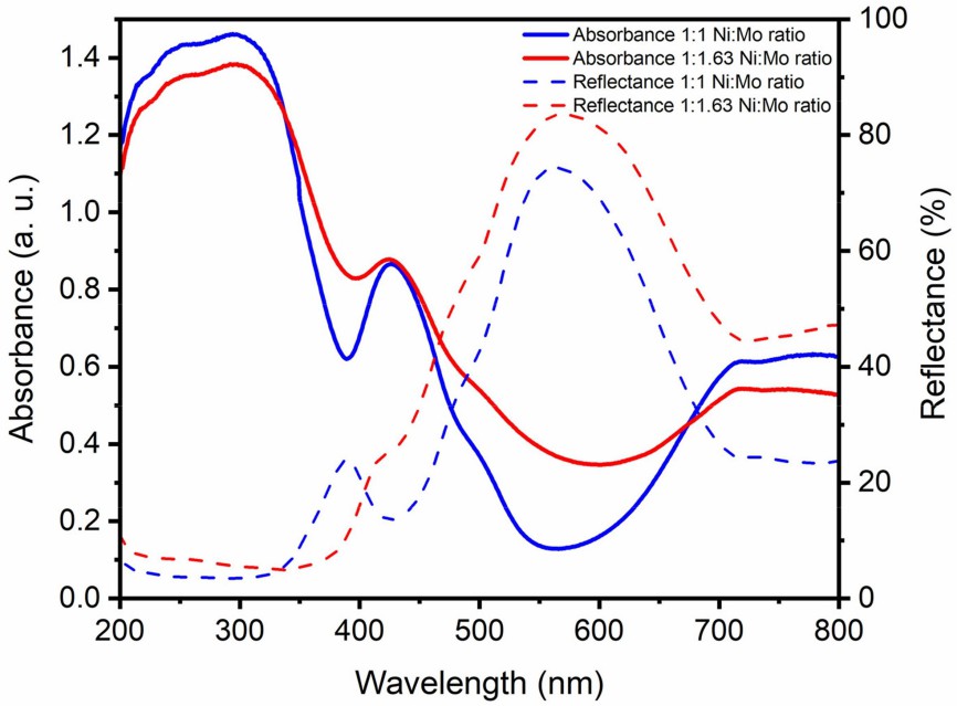
This study investigates the characterization of NiMoO4 powders as a semiconductor for potential photocatalytic applications. The materials were synthesized using a simple hydrothermal method, with varying Ni:Mo molar ratios (1:1 and 1:1.63). The structural and optical properties were extensively evaluated through X-ray diffraction, Raman spectroscopy, UV-VIS absorption, and diffuse reflectance spectroscopy, alongside photocatalytic tests for methylene blue removal under UV light.
UV-VIS spectroscopy revealed two key absorption edges in the NiMoO4 samples—one in the UV region around 350 nm, linked to the fundamental absorption edge, and another in the visible range near 425 nm, attributed to nanocrystalline NiMoO4. Notably, the sample with the 1:1.63 Ni:Mo ratio exhibited a broader absorption band, suggesting a significant effect of the Mo content on the material's optical properties.
The optical band gaps of the samples were calculated using Tauc plots, indicating a direct bandgap of 3.50 eV for the 1:1 Ni:Mo ratio and 3.11 eV for the 1:1.63 ratio. This variation highlights the influence of Mo incorporation on the material's electronic structure, which is critical for optimizing photocatalytic efficiency.
These results emphasize the importance of controlling the synthesis parameters, such as the Ni:Mo ratio, in tailoring the optical properties of NiMoO4 for enhanced photocatalytic applications.
 Luxová, Jana, et al. Materials Science and Engineering: B 313 (2025): 117889.
This study investigates the characterization of Mn-doped SrTiO3 perovskite, focusing on its potential as a visible light-active semiconductor for photocatalytic applications. The doping of manganese (Mn4+) was successfully integrated into the SrTiO3 structure, evidenced by X-ray photoelectron spectroscopy (XPS) and energy-dispersive X-ray (EDX) analysis. The material exhibited a dark brown color due to enhanced visible light absorption, with a significant reduction in the band gap from 3.32 eV to 2.92 eV, indicating improved photocatalytic activity.
Scanning electron microscopy (SEM) analysis revealed that both undoped and Mn-doped samples exhibited similar microstructures composed of submicron grains, with Mn uniformly distributed across the perovskite lattice. The adsorption capacity of Mn-doped SrTiO3 was tested using Methylene Blue (MB) dye at pH 10, showing a maximum removal capacity of 310.7 mg/g, slightly outperforming the undoped sample. This enhanced adsorption was attributed to electrostatic interactions between the material's surface and the dye molecules.
These results highlight the significant role of Mn-doping in tuning the optical properties and improving the material's photocatalytic efficiency. The findings underscore Mn-doped SrTiO3 perovskite's potential for environmental and energy applications, particularly in photocatalytic degradation processes under visible light.
Do not know how to place an order, please refer to the flow chart shown below.
Submit quotation request |
A technical manager will contact you within 24 hours |
You will review and approve the final price and place an order |
Confirm with you and make the payment |
Instruct you to ship your samples and form |
Analytic report delivery |
